Regarding photo-etching
Photo-etching technology is (separately called Photo Etching/Chemical Milling) a technology to cut and process metals by combining corrosion resistance masking that applies precision photographic technology and chemical cutting through the chemical reaction and corrosive action of metals. It is a dedicated technology that can respond to a precision process of ultra-small, ultra-thin and complicated shapes used in the electronics field, as well as a variety of other fields such as optics, electrics and electronics.
1. Technological characteristics of photo-etching
* Possible for ultra-fine, high density, complicated and ultra-small processing
* Possible to process the sheet thickness of a material, enabling grooving in an arbitrary shape, or process a protruding shape within the sheet thickness.
* No change in material occurs and no burrs, bends or deformation of a product occurs due to processing.
* Expensive mold or jig tools are not required, resulting in a drastic reduction in initial investment, as well as a reduction in delivery time.
* Possible to respond to time sensitive deliveries and small lot production runs. (Shortest delivery and lot: One day/one piece)
2. Processable materials:
Steinless / Copper / Copper alloy / Brass / Nikkel silver / phospher Bronze / Steel / Special steel / permalloy / other secial alloy
SUS, steel materials, special steel, carbon steel and permalloy
Non-ferrous metal (Copper, copper alloy, brass, albata, phosphor bronze)
Contact us regarding other materials, including special materials.
Special materials and difficult-to-process materials (titanium, magnesium, etc.) are also available. Please contact us directly.
3. Sheet thickness to be processed
t=0.005mm-Max1.5mm
Contact us for maximum processing width and longitudinal materials.
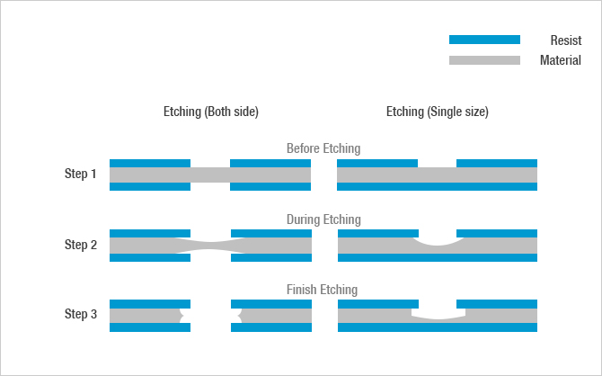
Etching processing progress image
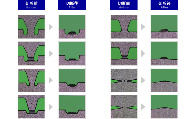
Bridge shape
During the etching process, the product needs a junction (bridge). An appropriate shape must be planned depending on sheet thickness and shape.
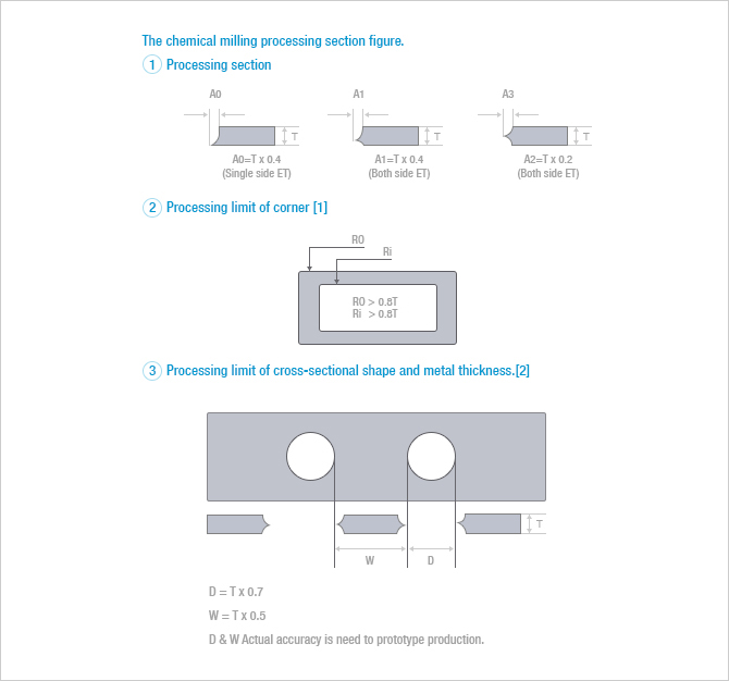
Process limitation and accuracy (Standard specification)
Major usage of etching products
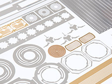
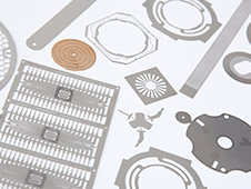
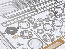
| Electrical parts | Earth plate, heater shield plate, antenna |
|---|---|
| Electronic parts | Conductors, terminals, evaporation masks, yokes, lead frames, metal masks, head cores |
| Parts for optical devices | VCM (leaf spring), shutter, aperture, douser, pinhole, optical diaphragm, field frame parts |
| Parts for OA devices | Leaf springs, grid plates, steel belts |
| Parts for measuring equipment | Spacers, encoder metal squeegees, shim cage |
| Precision parts | Filters, slits, springs, mesh |
| Other | Decorative things, meter related products, flow channels, diaphragms, jigs, parts for models, dial plates, reinforced plates, laminates, cases |